Supercapacitor Charging Circuitry
12/2025 – 3/2026
elevator pitch
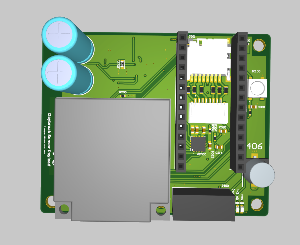
The Iridium 9603N modem draws about 6.5 W during a transmit burst, but our payload was only allowed 1.5 W continuous. Wired directly, the first transmission drags the 5 V rail down and browns out the radio. To fix this, I designed a two-cell series supercapacitor bank in Altium that separates average power from instantaneous power: it stores energy while the modem is idle, supplies the burst, then recharges under a current limit that keeps total draw inside the 1.5 W allowance. A state-of-charge lockout blocks transmission until the bank has recovered. The board flew on USC Rocket Propulsion Laboratory’s Daybreak vehicle in April 2026, which reached 331,790 feet.
core processes
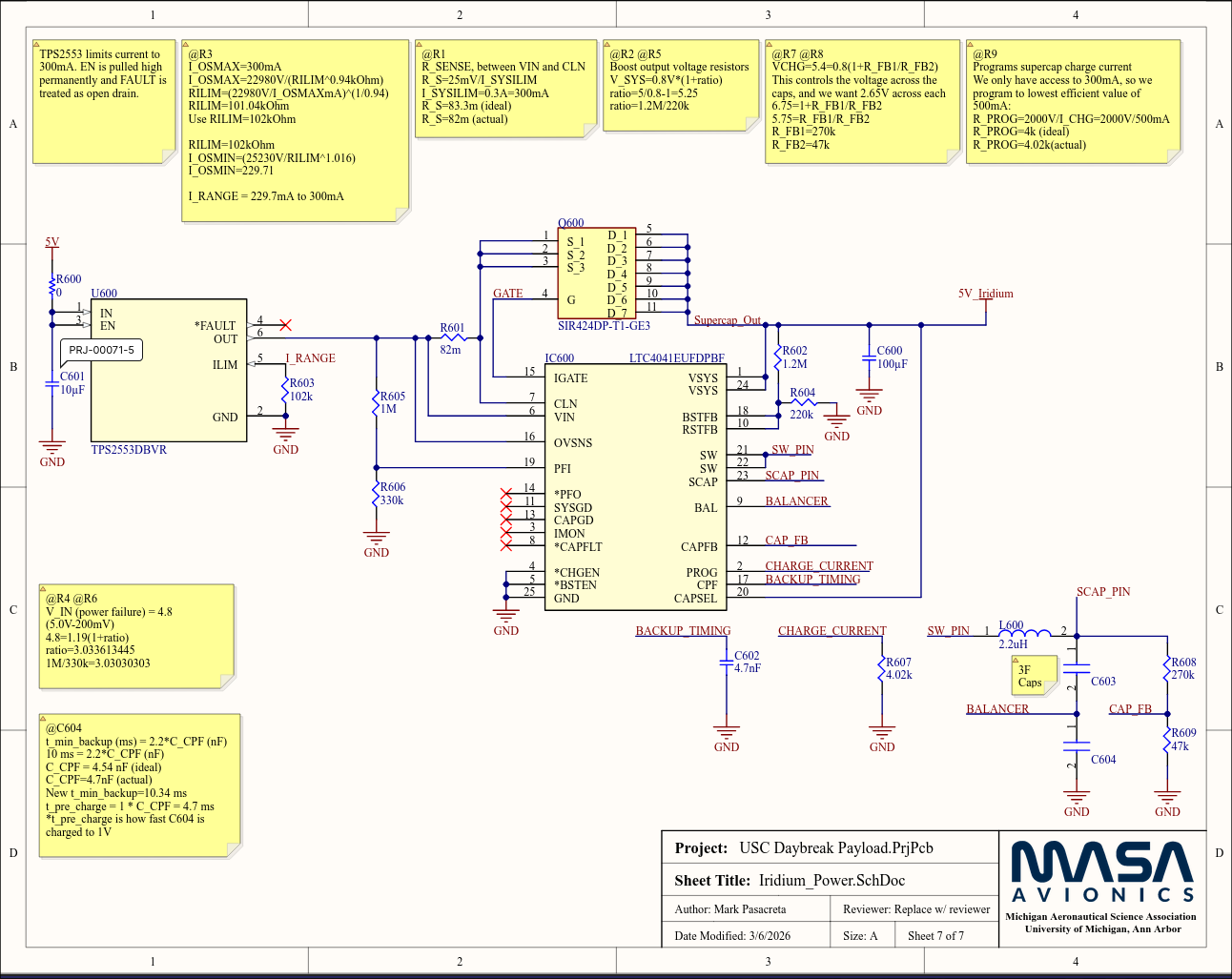
Two constraints drove the design. First, the 5 V rail cannot drop below 4.5 V, and a supercapacitor’s terminal voltage falls linearly as it discharges. So the real question is not whether the bank stores enough energy — it is whether the voltage stays above 4.5 V through the whole burst, including the drop across the bank’s own ESR. Second, the payload idles at about 200 mA at 5 V, which leaves only about 0.5 W to recharge with. That means every transmission needs a recovery period afterward, and it is why the lockout is necessary rather than optional.
Common supercapacitor cells are rated for 2.7 V, so a 5 V rail needs two in series, giving a 5.4 V maximum. Two series cells will not share voltage evenly on their own because of tolerance differences, so the bank needs active balancing — handled by the charger’s built-in balancer tied to the cell midpoint. The charge path also has to be current-limited, because an empty supercapacitor looks like a short circuit; without the limit, the payload would trip its upstream protection at power-up and never turn on. An LTC4041 supercapacitor charger manages the bank, with charge current set by its PROG resistor (4.02 kΩ, a 500 mA setting), behind a TPS2553 power switch that caps total input current at 300 mA.
The sizing came out somewhere unintuitive. Pulling 1.4 A for 8 ms out of roughly 1 F only removes about 11 mV of voltage against 900 mV of headroom. Almost all of the droop is ohmic — it comes from resistance, not from lost charge — so the right cell is chosen by ESR, not capacitance. The cell is Eaton’s HV0820-2R7305-R: 3 F and 2.7 V, rated at 80 mΩ maximum ESR. Two in series make a 1.5 F bank (roughly 1 F after tolerance and aging) with up to 160 mΩ of ESR — about 220 mV of ohmic drop at 1.4 A, and still under 450 mV even at the datasheet’s end-of-life limit of double the initial ESR.
results and improvements
I wrote the hardware qualification protocol for the board. Random vibration ran at 6.8 Grms for 5 minutes on each of three orthogonal axes, with a 20–2000 Hz profile: 0.01 g²/Hz at the endpoints, ramping at +3 dB/octave up to a 0.04 g²/Hz plateau from 80 to 500 Hz, then rolling off at −3 dB/octave. Thermal cycling ran four cycles from −28 °C to +40 °C (±2 °C) at 3 °C/min with 30-minute dwells. The board passed both, and it passed functional tests through integration and pre-flight.
I shipped the qualified board to USC RPL in March 2026, which closed out my part of the project; integration and flight operations were in their hands from there.
The payload returned no data from the flight. The failure was in firmware — the root cause was never determined on my end, since the board left my hands at the March handoff — but the power hardware worked through pre-flight testing and was not the cause.
The main improvement would be instrumentation. The buffer records nothing about itself, so when the firmware failed downstream, there was no independent record of whether the power system did its job. Logging the bank voltage and lockout state onboard — or even adding a latching brownout supervisor readable on the ground — would have made the board’s own performance recoverable without depending on the software that failed.